By Gary Tharalson, Motorola, Inc., Mesa, AZ
Introduction
When a logic designer is faced with developing a new product requiring
performance significantly different from the past, it might be well to examine
various logic family alternatives. Selecting a logic family for a new design
from today' s rapidly changing semiconductor technologies can be a perilous
task. With the many choices available, it is easy to under-kill or over-kill an
application with inadequate or excessive capabilities.
By selecting the family whose parameters most closely fit your needs, you
can save many future headaches. Obviously, before selecting a specific device, a
detailed review of the vendor' s data sheet specifications is recommended.
Family Comparison
The table below compares some typical characteristics of several popular
logic families available in the market today. The following sections provide
brief explanations of the various parameters.
| Typical Commercial Parameter (0°C to +70°C) |
Logic Families | ||||||||||||
|---|---|---|---|---|---|---|---|---|---|---|---|---|---|
| TTL | CMOS | ECL | |||||||||||
| LS | ALS | ABT | FAST | MG | HC | FACT | LVC | LCX | 10H | 100K | ECL in PS(3) |
E-Lite | |
|
Speed Gate Prop Delay (ns) Flip-Flop Toggle Rate (MHz) Output Edge Rate (ns) |
9 33 6 |
7 45 3 |
2.7 200 3 |
3 125 2 |
65 4 50 |
8 45 4 |
5 160 2 |
3.3 200 3.7 |
3.5 200 3.6 |
1 330 1 |
0.75 400 0.7 |
0.33 1,000 0.5 |
0.22 2800 0.25 |
|
Power Consumption Per Gate (mW) Quiescent Operating (1 MHz) |
5 5 |
1.2 1.2 |
0.005 1.0 |
12.5 12.5 |
0.0006 0.04 |
0.003 0.6 |
0.0001 0.6 |
0.003 0.8 |
1E-04 0.3 |
25 25 |
50 50 |
25 25 |
73 73 |
|
Supply Voltage (V) |
+4.5 to +5.5 |
+4.5 to +5.5 |
+4.5 to +5.5 |
+4.5 to +5.5 |
+3 to +18 |
+2 to +6 |
+1.2 to +3.6 |
+2 to +3.6 |
+2 to +6 |
-4.5 to -5.5 |
-4.2 to -4.8 |
-4.2 to -5.5 |
-4.2 to -5.5 |
|
Output Drive (mA) |
8 |
8 |
32/64 |
20 |
1 |
4 |
24 |
24 |
24 |
50 ohm load |
50 ohm load |
50 ohm load |
50 ohm load |
|
5V Tolerant Inputs Outputs |
N/A N/A |
N/A N/A |
N/A N/A |
N/A N/A |
N/A N/A |
N/A N/A |
N/A N/A |
Yes No |
Yes Yes |
N/A N/A |
N/A N/A |
N/A N/A |
N/A N/A |
|
DC Noise Margin (1) High Input % Low Input % |
22 10 |
22 10 |
22 10 |
22 10 |
30 30 |
30 30 |
30 30 |
30 30 |
30 30 |
27 31 |
41 30 |
28/41 31/31 |
33 33 |
|
Packaging(4) DIP SO LCC SSOP TSSOP |
Yes Yes No No No |
Yes Yes Yes Yes No |
Yes Yes No Yes No |
Yes Yes Yes Yes No |
Yes Yes No No Yes |
Yes Yes No Yes Yes |
Yes Yes Yes Yes Yes |
No Yes No Yes Yes |
No Yes No Yes Yes |
Yes No Yes No No |
Yes No No No No |
No No Yes No No |
No Yes No No No |
| Functional devices Types | 190 | 210 | 50 | 110 | 125 | 103 | 80 | 35 | 27(2) | 64 | 44 | 48 | 40 |
|
Relative 1-25 Gate Price U.S. $ |
.90 | 1.00 | 1.60 | 1.00 | .90 | .90 | 1.50 | 1.80 | 1.80 | 2.00 | 10.00 | 28.00 | 32.00 |
(1)Typical noise margin expressed as a percentage of
typical output voltage swing.
(2)Announced plans for Motorola offering.
(3)ECLinPS
is available in both 10H and 100K compatible versions.
(4)A "Yes"
may not include all devices within a family.
Manufacturers Data Books Referenced:
Motorola, DL121, DL122, DL129,
DL131, DL138, DL140, BR1339
Texas Instruments, SDAD001B
Phillips
Semiconductor, IC23, IC24
National Semiconductor, F100K
Logic Families
Although there are many family technologies
available, they can be divided into roughly three broad categories:
Transistor-Transistor Logic (TTL), Complementary Metal- Oxide Semiconductor
logic (CMOS), and Emitter-Coupled Logic (ECL). TTL and ECL are bipolar
technologies differing in implementation techniques, while CMOS (an MOS
technology) differs in fundamental transistor structure and operation.
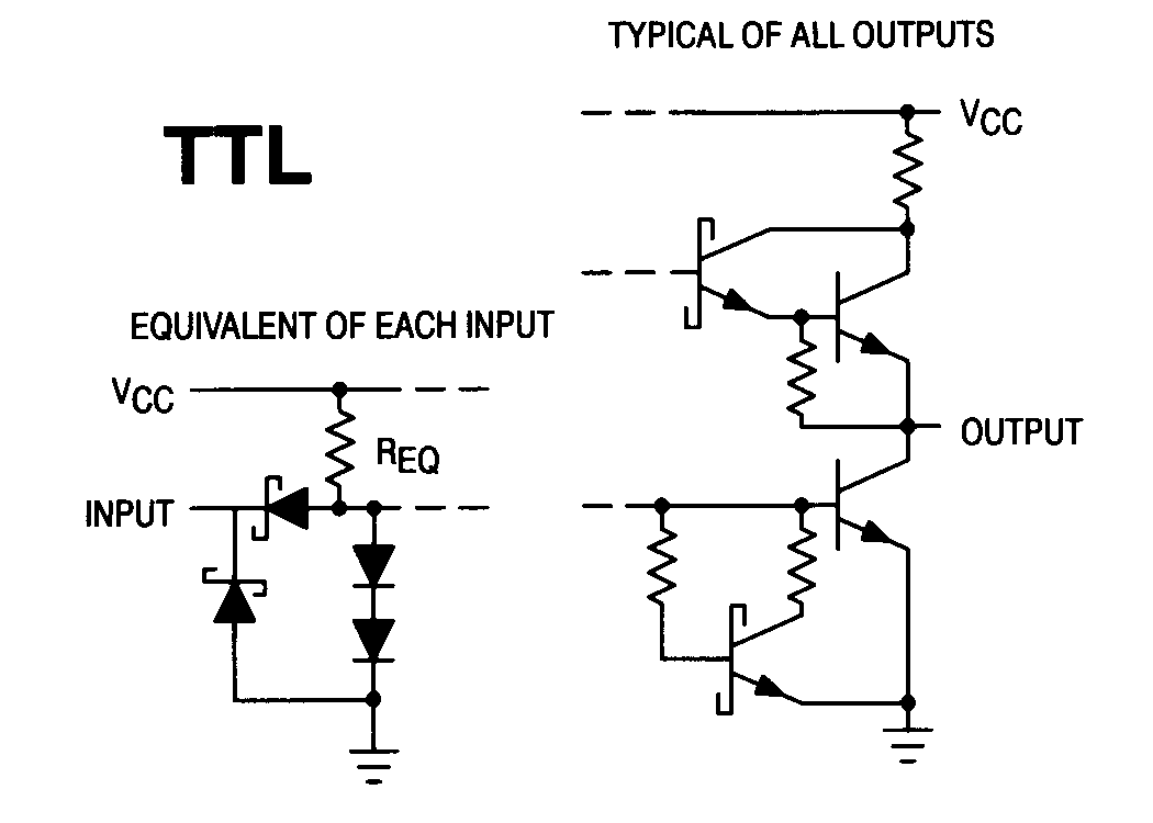
TTL
The designation " bipolar" essentially refers to
the basic component utilized to build this family of integrated circuits, the
bipolar transistor. By employing a bipolar transistor in a logic function' s
output driver as well as the input buffer, it results in a
Transistor-to-Transistor (TTL) direct connection. Older technologies were
interconnected via passive components such as resistors or diodes.
Since the original TTL design, several enhancements have been employed to reduce power and increase speed. Common to these has been the use of Schottky diodes which, ironically, no longer result in strictly TTL connections. Consequently, the two names, Schottky and TTL, are used in combination: LS (Low power Schottky), ALS (Advanced Low power Schottky), and FASTTM (Advanced Schottky) TTL.
The superior characteristics of TTL compared to CMOS, in the past, have been its relatively high speed and high output drive; these advantages are rapidly diminishing as described in the next section. One family of devices, ABT (Advanced BiCMOS Technology), utilizes TTL circuitry at the inputs and outputs, and CMOS technology in between--attempting to combine the advantages of both bipolar and CMOS.
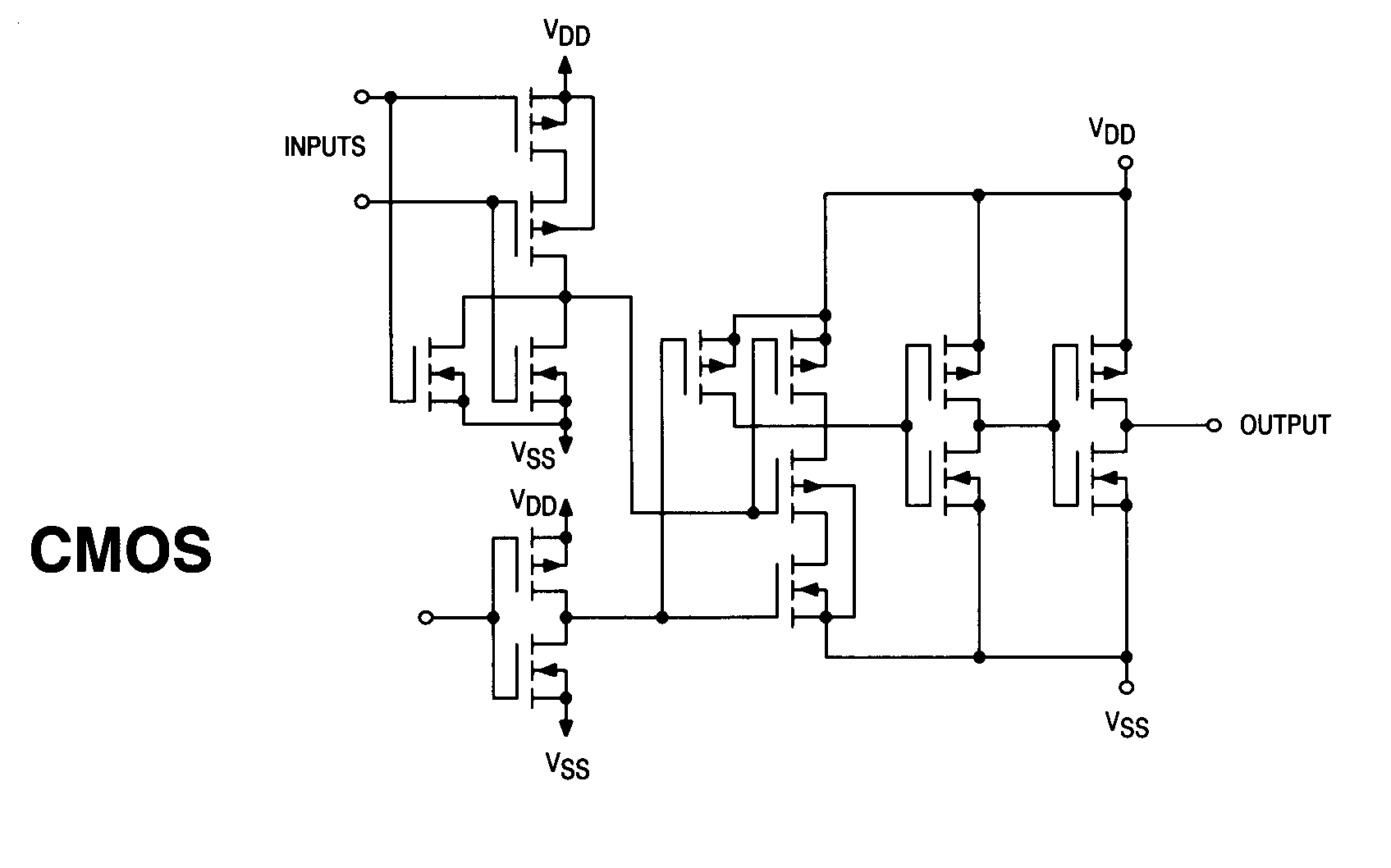
CMOS
Complementary Metal-Oxide Semiconductor (CMOS) field-effect
transistors differ from bipolar both in structure and operation. The primary
advantages of CMOS are its low power dissipation and small physical geometry.
Advances in design and fabrication have brought CMOS devices into the same speed
and output drive capability as TTL. Again, enhancements have resulted in the
evolvement of additional classifications: MG (Metal-Gate CMOS), HC (High-speed
silicon-gate CMOS), and FACTTM (Advanced CMOS).
The most recent evolution in CMOS logic has been in reducing supply voltage
without sacrificing performance. The new LCX family is one outgrowth of this
trend. This family results from the joint efforts of a triumvirate of companies
including Motorola, National, and Toshiba. Although each company has done its
own design and fabrication, they have mutually agreed to provide identical
performance specifications. In addition to the 3V operating voltage, LCX inputs
and outputs are tolerant of interfacing with 5V devices.
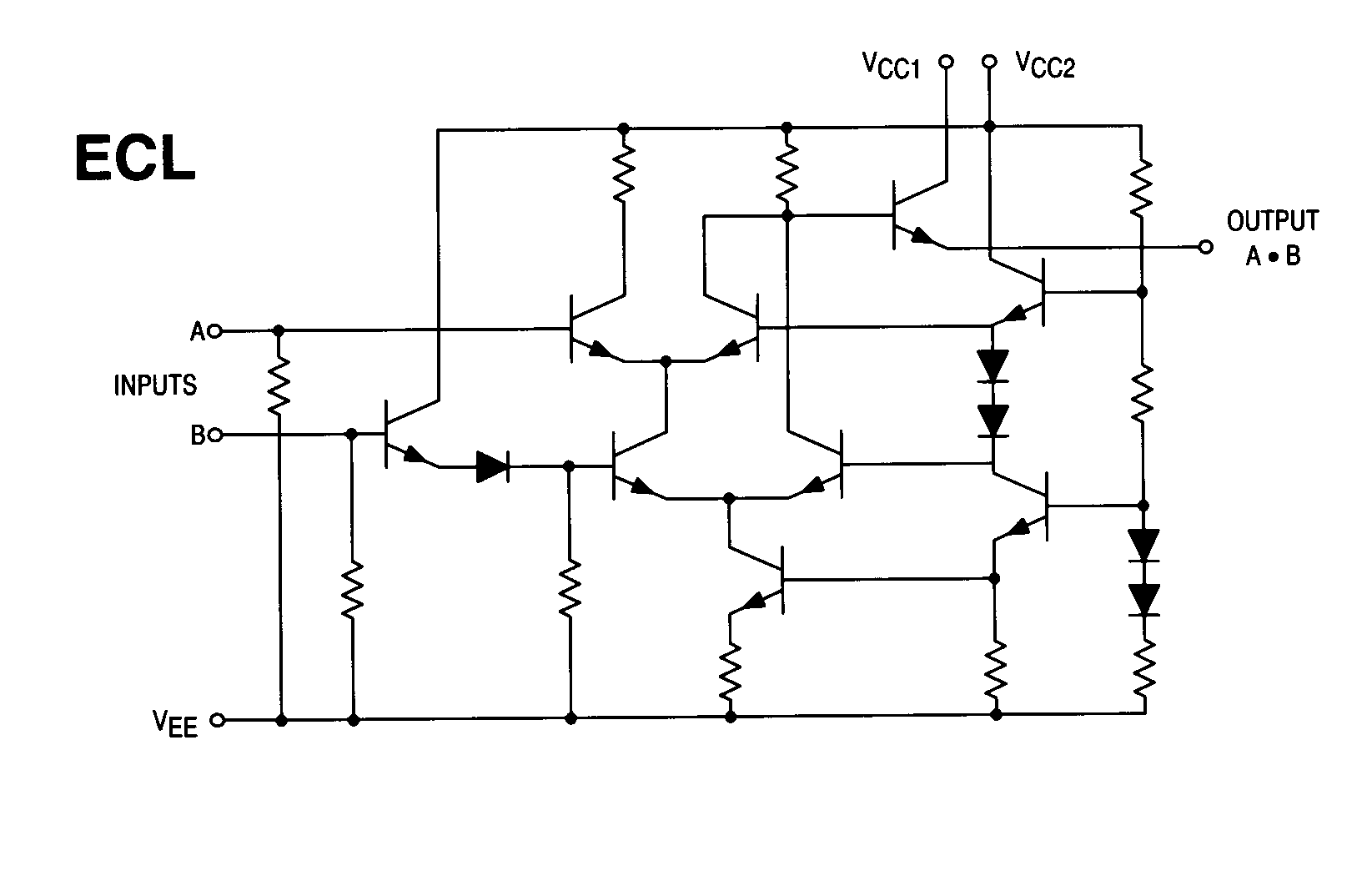
ECL
Emitter-coupled logic (ECL) derives its name from the
differential-amplifier configuration in which one side of the diff-amp consists
of multiple-input bipolar transistors with their emitters tied together. An
input bias on the opposite side of the diff-amp causes the amplifier to operate
continuously in the active mode. Consequently, ECL consumes a relatively
substantial amount of power in both states (one or zero) but also results in the
fastest switching speeds of all logic families. An inherent benefit of ECL is
the narrow switching level swing between devices (approximately 800 mV) which
helps to reduce noise generation.
There have also been many evolutionary advancements in ECL, the following
being some of the most prominent: 100K (1975), 10KH (1981), and ECLinPSTM (1987). Of most recent vintage is the ECLinPS LiteTM family of single function devices. By focusing on
simplicity, this family achieves very high performance, while at the same time
reducing package size.
Speed
Speed is typically the first parameter at which a designer
looks, and when design engineers are asked what features of a logic family they
would like enhanced, usually they want more speed. But increased speed often
brings along many potential problems such as: increased noise generation, higher
power consumption, increased component and system cost, more difficult board
layout, etc. An assessment of the other family parameters is usually required
before a final selection is possible.
In Table 1. , family speed is compared for three parameters using typical
values: propagation delay through a simple OR gate, flip-flop toggle frequency,
and output switching time. Typical values can be misleading as they are
frequently specified according to different vendor' s criteria, but they are
usually close to an average of min and max values. For final assessment of a
particular component' s performance, the min/max spec' s provided in most
vendor' s data sheets should be examined. Furthermore, switching (edge) rate is
highly load dependent, and again, data sheet specifics must be compared.
Power Consumption
The amount of power an application consumes (and
the subsequent heat generated) is frequently of prime importance. One of the
major differences between the three families, the power parameter may also limit
the designer' s choices.
TTL consumes a moderate amount of power and is nearly constant over operating frequencies up to about 10 MHz; above 10 MHz it begins to climb rapidly. Although only a few milliwatts are consumed by each device, in a complete system a substantial amount of power may be used.
CMOS power consumption, on the other hand, is highly frequency dependent. In quiescent mode (zero frequency), it consumes almost no power at all, being measured in microwatts/device. However, its consumption grows almost linearly with frequency so that at maximum operating frequency it may be several milliwatts/device. The great power reduction advantage of CMOS derives from the fact, that in most applications, the percentage of the total number of devices operating at high frequencies at any given time is small; consequently, the average total power consumed by the system is greatly diminished.
Since power consumption is proportional to the square of supply voltage,
simply reducing the operating voltage will have desirable effects.
Unfortunately, speed generally falls off as well. By designing the LCX family
specifically for a lower supply voltage, it was possible to maintain high
overall performance. The LCX family is also designed to interface with five volt
devices, being tolerant of the differences in I/O levels. Because of its
inherent design, ECL is the highest power consumer at frequencies below
approximately 50 MHz; however, at higher frequencies, TTL and CMOS power
consumption can exceed ECL. The amount of power used by ECL is fairly constant
over its entire operating frequency range. Designers of large, high performance
ECL systems may have to employ somewhat more complex cooling and power
distribution techniques.
Supply Voltage
The power supply voltage required for TTL and ECL is
restricted to fixed values; only a narrow voltage variation is allowed for the
device to remain within specifications. Since these families also consume
substantial amounts of power, there is a large current flow through the power
lines. To avoid unacceptable voltage fluctuation, various preventive measures
may be necessary such as remote sensing by the supply regulator, beefing up
power buses and filters, and utilizing multi-layer PC boards with separate power
and ground planes. Typically, a high-speed energy storage capacitor is required
near each logic device; this capacitor maintains the correct device voltage
during high-current switching.
An important advantage of CMOS is the large range of supply voltage over
which operation is specified. By allowing systems to be operated at voltages as
low as 2V, not only is power consumption lowered, but noise generation from fast
signal switching is reduced. It must be noted, however, that operating speed
drops off rapidly as the voltage is reduced. As mentioned previously, this was a
significant reason for developing the LCX family.
Output Drive
An important characteristic of a logic device is its
ability to drive relatively large loads without significant speed degradation.
The older families within TTL, and especially CMOS, had only limited drive
capability (below 10 mA). All advanced logic family versions have significantly
increased drive capacity, and several (FACT, LCX and all ECL) are capable of
driving 50 ohm transmission lines directly. Furthermore, because of the
symmetrical sink/source capability of FACT and LCX, their rise and fall times
are nearly equal, resulting in balanced delay times.
5V Tolerant Input/Output
Because of the limited number of functions
available in the new low voltage CMOS families, a designer might might have to
mix 3V and 5V devices, each operating from 3V and 5V rails, respectively. Unless
the 3V device was specifically designed with proper protection to tolerate 5V at
its input or output, it may not survive.
Noise Margin
Noise immunity refers to the resistance of a logic
device to undesired switching. Depending on the input level, a noise glitch that
causes a transient across the input switch point from either a high or low level
can result in erroneous operation. Clearly, the more voltage difference there is
between the switch point and the normal input high and low levels, the more
immunity a logic family has to erroneous switching. In Table 1. , these
differences are expressed as a percentage of the swing between typical output
high and low voltage logic levels. High input noise margin is calculated from
the formula: HNM = VOH-VIH over VOH-VOL. Low input noise margin is calculated
from the formula: LNM = VOH-VIH over VOH-VOL.
Packaging
The venerable Dual-Inline package (DIP) is rapidly being
replaced by Small Outline (SO), Shrink Small Outline (SSOP), Thin Shrink Small
Outline (TSSOP), and Leadless Chip Carrier (LCC) packages for surface mounting.
Savings in footprint area of up to 90% are possible with these newer packages.
Device Types
In general, the older the family the larger the
quantity of different functional devices available. This is only natural since
it takes time (and substantial resource investment) to design and reliably
manufacture increasingly more complex devices. The newer TTL and CMOS families
will undoubtedly grow, but because of competition from higher integrated
devices, will be more limited in scope.
Cost
Here again, the age of a family has a substantial bearing on
its relative selling price. The older families have benefited longer from
manufacturing learning and volume curve cost reductions. Newer technologies,
because of their inherently more complex process requirements, increased
performance improvements, and higher cost of production, are priced higher but
should decline over time.
Mix and Match
Many designers have found that the best approach to
achieving their particular application performance goal is to combine devices
from several families. The obvious advantage of this is to optimize the
requirements of selected portions of a design, whether it is for speed, power
consumption, output drive, cost, etc. Some disadvantages are that devices must
be analyzed and tested for compatibility, inventories may increase, and some
performance parameters may be compromised.
Conclusion
The diversity of logic families available to today' s
logic designer may be likened to a bad news/good news scenario. The bad news is
that you have huge ratios between the highest and lowest performance
values--speeds of 500:1, power at 100,000:1, output drive at 24:1, etc. The good
news is that you have lots of choices--it wasn' t too many years ago that there
were very few. By examining and comparing each family' s parameters, an optimal
selection can result.
A few potential users of standard logic devices may worry, that because of
the trends towards higher-integration chips, some vendors will abandon the older
product lines. This may eventually happen; however, the current demand,
projected for at least the next decade, indicates that these families have a
very solid future. The diverse applications that keep arising for semiconductor
products that are inexpensive and reliable continue to mount. Until some totally
revolutionary development should occur, these " oldies, but goodies"
will be around for a long time to come.
© Copyright 1996, Motorola, Inc. All rights reserved.
Last
Update: 09/10/96 JB