|
Electrical Design
The following are the design of our
electrical system. Please note that
you could download the Protel schematic from our download
section.
Please also see detail about our
port extension chip (P8255) at the end of this page.
Main Circuit
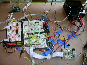
Diagram
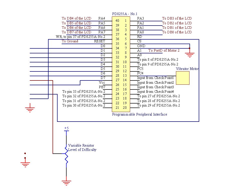
Figure
1
Main Wiring Diagram
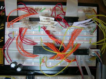
Figure 2 and 3 show the zoom views
of the main wiring diagram
Figure
2
Zoom on the left side of the Main Wiring Diagram
Figure
3
Zoom on the right side of the Main Wiring Diagram
The following diagrams show the wiring of the
sub modules in the system.
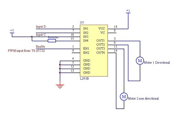
Figure
4
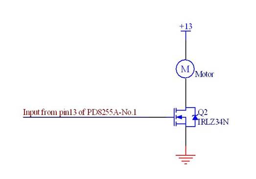
Wiring of the spinning motors
Figure
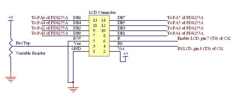
5
Wiring of the LCD
Figure
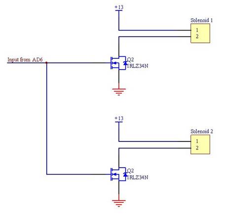
6
Wiring of the solenoid
Figure
7
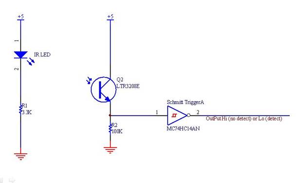
Wiring of the Passing Point
Calculating R1 value
From Vf of the LED ≈ 1.2 V
Current pass through the LED =  = =  =
1.15mA < 100 mA max rated current =
1.15mA < 100 mA max rated current
Calculating R2 value
From trial and error to ensure that
the current from 3208E is sufficient to trigger the Schmitt Trigger
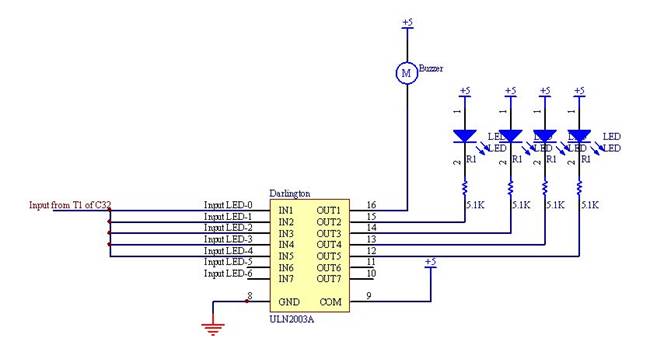
Figure
8
Wiring of the LED flasher and buzzer
Calculating R1 value
From Vf of the LED ≈ 1.2 V
Current pass through the LED = =  = =
 =
0.57mA < 100 mA max rated current =
0.57mA < 100 mA max rated current
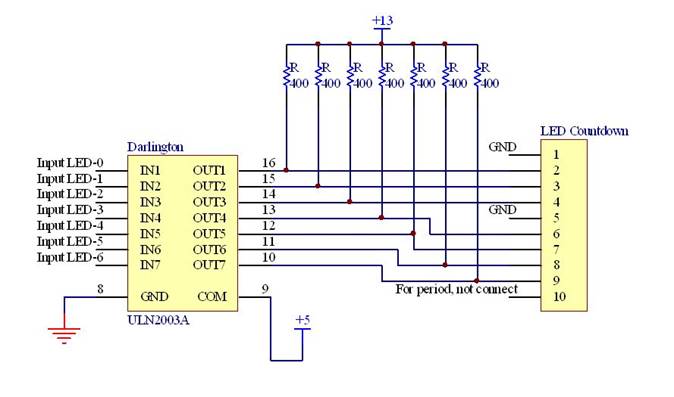
Figure
9
LED digit countdown timer wiring
Calculating R value
From Vf of the LED ≈ 2.4 x 4
= 9.6 V
Current pass through the LED = =  = 8.5mA < 40 mA max rated current = 8.5mA < 40 mA max rated current
Figure
10
Vibrating Motor wiring
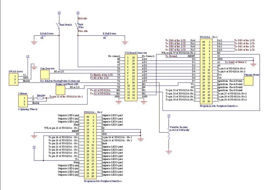
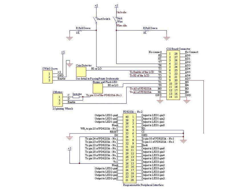
P8255
(Port Extension Chip)
Purpose: Since C32 board
does not have enough input/output pins for the project, we used the P8255
chip as a port extension chip. Basically,
P8255 extends the 8 pins to 24 pins. However, the P8255 needs some control
signals, write enable, read enable, and two address signals. So the chip actually extends 11~12 pins
to 24 pins (twice as much). We
chose P8255 because of its high performance, popularity, and excellent
stability.
Usage: The usage of P8255
is identical to simple memory chip. P8255 has one 8 bit data port for data
transfer from and to the main micro processor. It has three 8 bit output ports, PortA,
PortB, and PortC. All output ports
can be used as input ports by configuring the chip (the ‘control word’ is
used for this configuring). Before
using the chip, the user has to send the control word to the chip to initialize
this chip, except that only simple control word is required.
Input Operation
|
A1
|
A0
|
RD
|
WR
|
CS
|
Description
|
|
0
|
0
|
0
|
1
|
0
|
PortA ->
DataBus
|
|
0
|
1
|
0
|
1
|
0
|
PortB ->
DataBus
|
|
1
|
0
|
0
|
1
|
0
|
PortC ->
DataBus
|
Output Operation
|
A1
|
A0
|
RD
|
WR
|
CS
|
Description
|
|
0
|
0
|
1
|
0
|
0
|
DataBus
-> PortA
|
|
0
|
1
|
1
|
0
|
0
|
DataBus
-> PortB
|
|
1
|
0
|
1
|
0
|
0
|
DataBus
-> PortC
|
|
1
|
1
|
1
|
0
|
0
|
DataBus
-> Control word
|
|